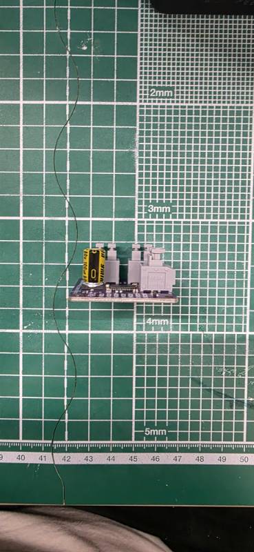
Circuit board
Model details
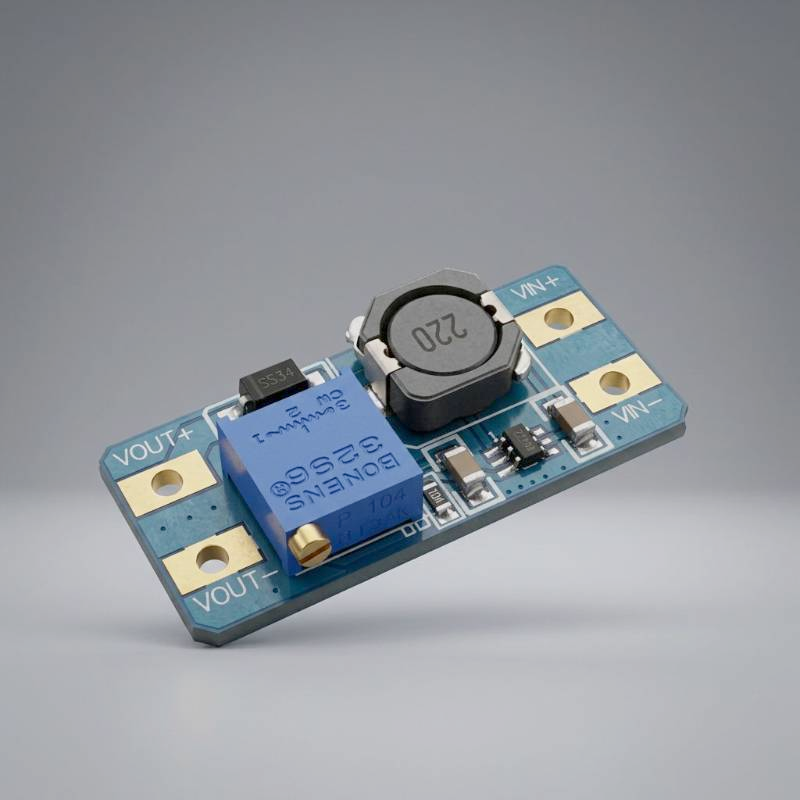
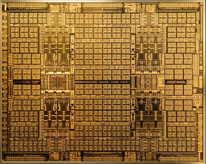
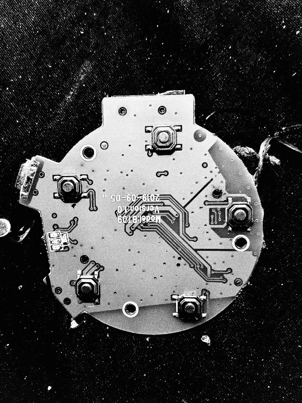
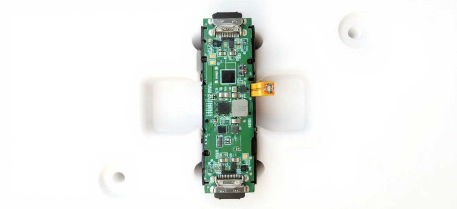
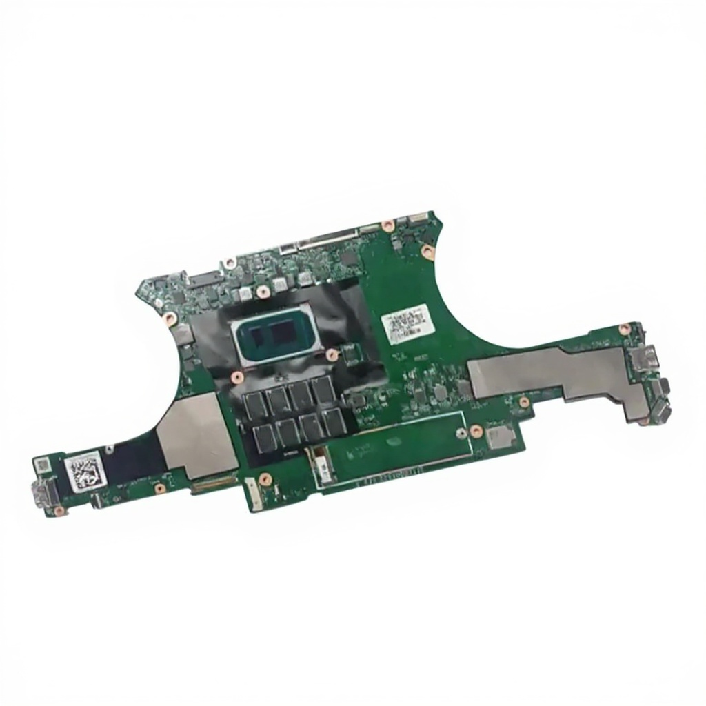
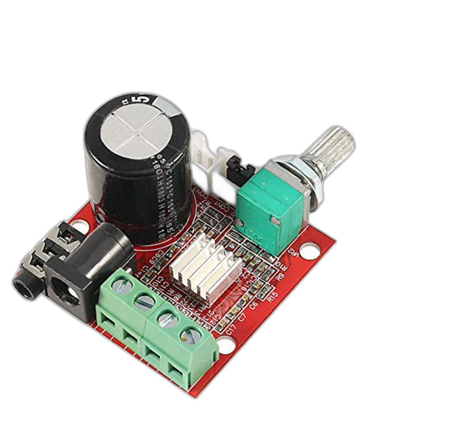
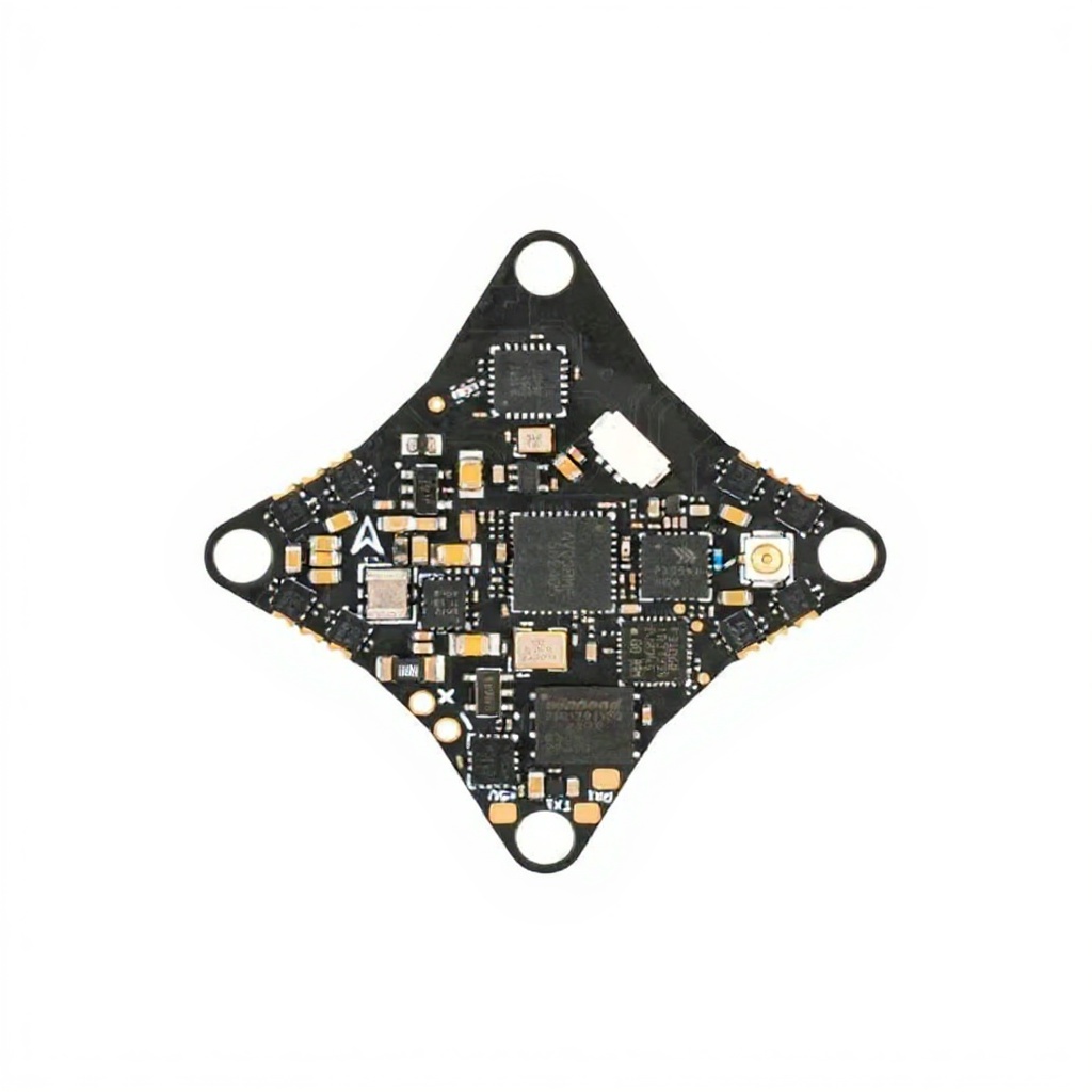
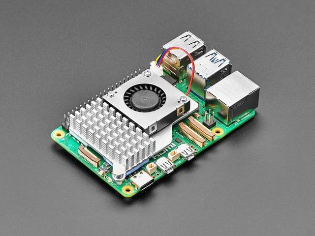
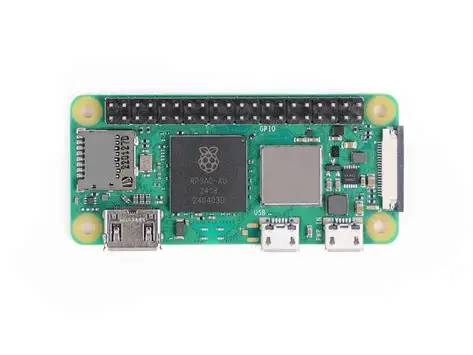
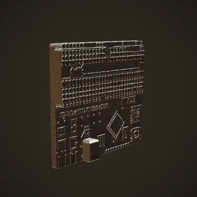
The image is effectively lit by directional lighting from the top left, casting strong shadows on the right and bottom right, enhancing visibility of the circuit board’s components. The board is positioned at an angle, angled slightly downward and to the right, allowing clear visibility of solder joints and component placement. The image is sharp and detailed, focusing on the circuit board’s texture and metallic components.
Use a similarly clear source photo to get a similar result. Generate yours →
Circuit board
Model details
The image is effectively lit by directional lighting from the top left, casting strong shadows on the right and bottom right, enhancing visibility of the circuit board’s components. The board is positioned at an angle, angled slightly downward and to the right, allowing clear visibility of solder joints and component placement. The image is sharp and detailed, focusing on the circuit board’s texture and metallic components.
Use a similarly clear source photo to get a similar result. Generate yours →